What Is Involved in the PCB Fabrication Process?
The rising demand for companies to adopt IoT or the Internet of Things is requiring intensive PCB fabrication processes. The PCB market expects to grow at a CAGR of 3% by 2024.
The PCB fabrication process assembles circuit boards for computers and electronic devices. This guide will show you everything you want to know in designing and manufacturing these units.
Contents
Printed Circuit Board
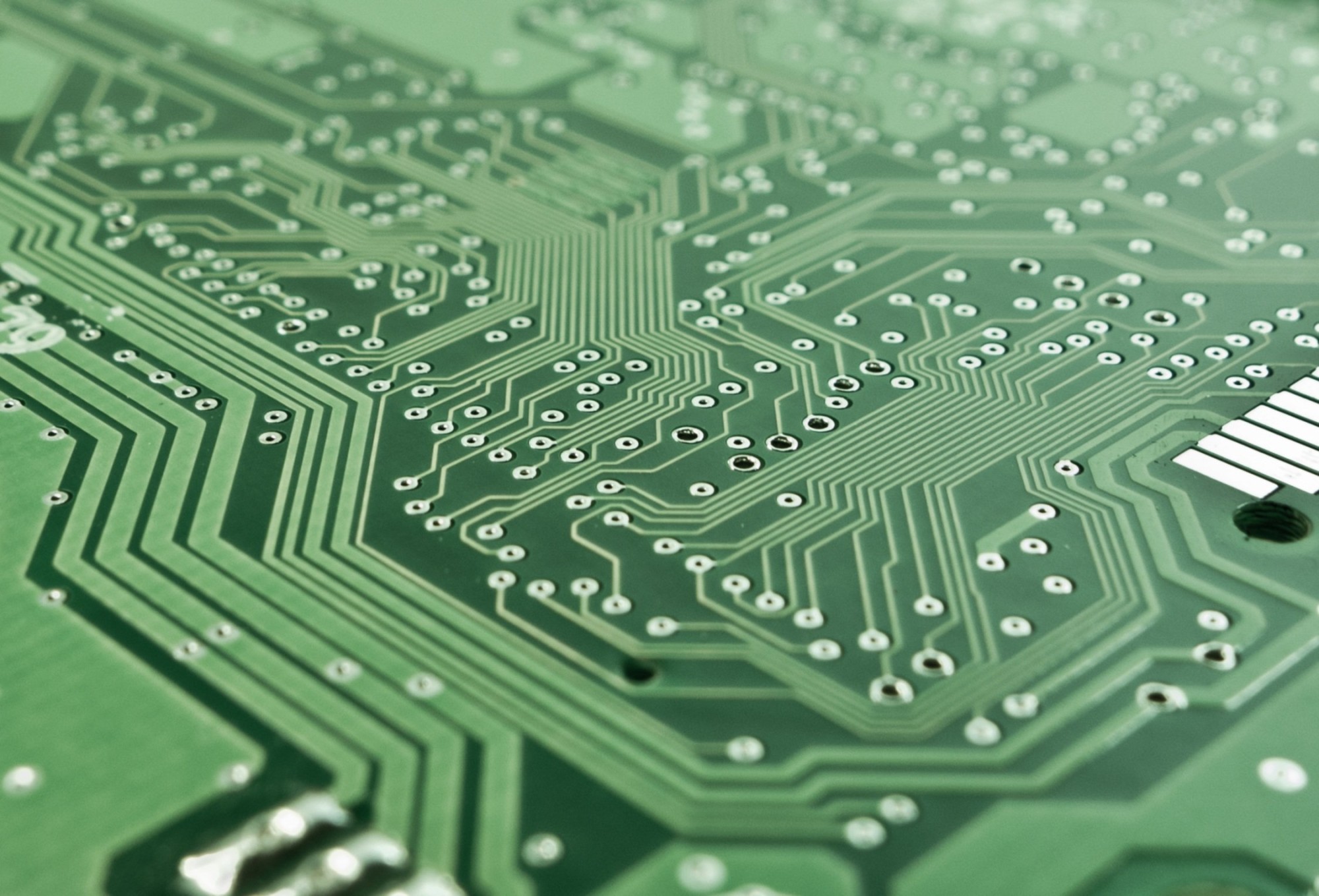
PCB is an abbreviation for the Printed Circuit Board. The Printed Circuit Board manufacturing process revolves around designing and assembling these circuit boards. These boards will serve as the foundation for the electronic device.
Certain companies will allow clients to upload a file with build specifications. This file, known as the Gerber file, provides a personal customary design. You can attain a PCB online quote to set the parameters of your PCB.
PCB engineers inspect any new orders filed with their respective companies. They have to make sure that these orders meet specifications.
This circuitry layout must be accurate. If there is a single component that does not abide by the complete schematics, it will harm the integrity of the board.
Steps of the Fabrication Process
The first step is to transfer the circuitry design to the board. Some PCB clients request a personal custom design.
Companies generate this design through photo tooling and direct imaging. There are two different methods of recreating this design:
A precision photo plotting tool, known as photo tooling, provides a template of the circuit layout on film. The company prints this layout or design.
The laser printing machine, through a process called Direct Imaging, prints the circuitry images onto the board.
These circuit boards contain many layers within the board that connect. The manufacturing process involves printing these designs outside and inside the core of the board as well.
This design prints onto a copper foil. A laminate board receives the copper that will inevitably contain the PCB design. This board goes through a decontamination machine to cleanse the material.
Inner and Outer Layers
A photo-resist layer presses against the board, UV light hardens and bonds the resist to the board. An alkaline solution removes the extraneous photo-resist material. This solution also removes any extra pieces of unnecessary copper.
Registration holes ensure all the layers of the board align. An optical inspection process occurs, comparing the layout to the original sketch.
Once all layer inspections are clear, it is time to start the layer-up and bond process. This essentially sandwiches all the pre-set layers together.
All pins and layers restraining the board together are then taken off. What emerges, is a complete board set for drilling.
An X-Ray locator aids in drilling precise holes across the circuit board. This can contain over one hundred and fifty bore intact points.
After drilling, the boards are brought through a chemical bath that adds a layer of copper to the surface panel.
After re-applying the photo-resist and plating, a surface finish and silkscreen apply a coating to the board. Thus, creating a complete board. The final steps involve soldering and testing the electronic overlay of the board before shipping.
Fabrication Process
There is a surprising amount of work that goes into the fabrication process. Each team member must analyze each step to ensure quality.
Companies are evolving as we are now able to mass-produce these boards through high-level machinery. Check out our software blog for more information on how to design and produce your own PCB.
Comments are closed.